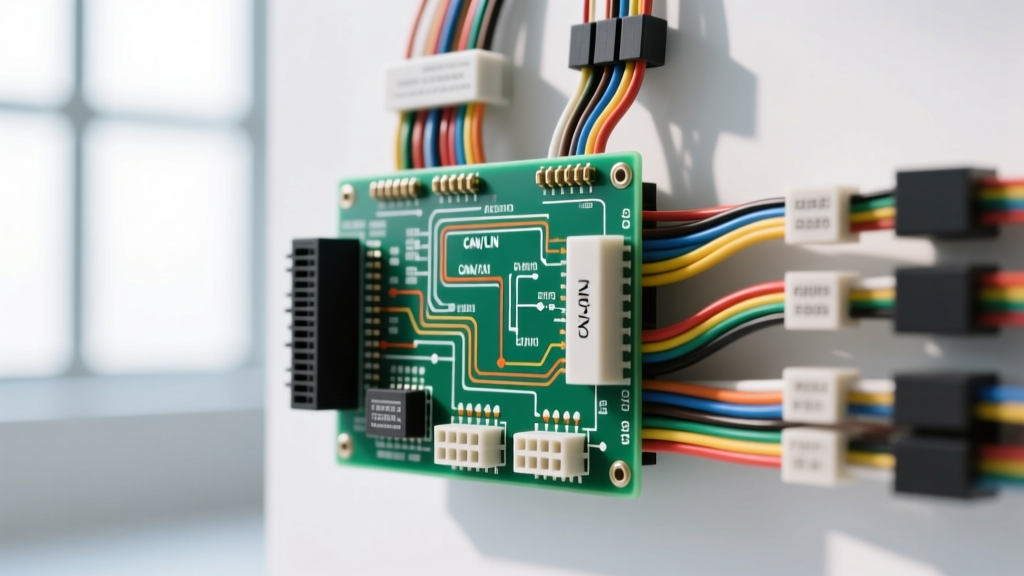
Architectural Overview: The BCM Block Diagram
The Body Control Module (BCM) serves as the central nervous system for a modern vehicle's chassis, comfort, and lighting electronics. While standard point-to-point schematics are invaluable for tracing a single broken wire, they fail to illustrate the logical relationships between multiplexed networks, power gating domains, and microcontroller subsystems. When technicians need to bridge the gap between physical wire routing and logical network mapping, they rely on a comprehensive wiring diagram body control module block diagram to isolate complex multiplexing faults and gateway communication errors.
A block diagram abstracts the BCM into functional zones: the Power Distribution Matrix, the Network Transceiver Hub (CAN/LIN/GMLAN), the Discrete Input/Output (I/O) Processors, and the High-Side/Low-Side FET (Field Effect Transistor) Drivers. Understanding this macro-architecture is critical for diagnosing intermittent bus failures, parasitic draws, and module logic lockups on platforms like the GM GMT900 and Ford F-150 architectures.
Network Topology and Bus Architecture
The BCM acts as a central gateway, translating high-speed powertrain data into low-speed body network commands. In a typical block diagram representation, the network transceiver hub is shown interfacing directly with the microcontroller's SPI or internal CAN controller.
High-Speed and Low-Speed CAN/GMLAN Domains
Modern BCMs manage multiple differential bus pairs. The block diagram delineates the physical layer transceivers from the logical data link layer. For example, on General Motors' GMLAN (GM Local Area Network) architecture, the BCM bridges the High-Speed GMLAN (500 kbps) and the Low-Speed GMLAN (83.3 kbps or 125 kbps).
- CAN-H / GMLAN+: Typically routed as a Dark Green (DK GRN) 18 AWG wire. Recessive state sits at ~2.5V, dominant state drives to ~3.5V.
- CAN-L / GMLAN-: Typically routed as Dark Blue/White (DK BLU/WHT) 18 AWG wire. Recessive state sits at ~2.5V, dominant state drives to ~1.5V.
- Termination Resistors: The block diagram will explicitly note the internal 120-ohm termination resistors located within the BCM and the Engine Control Module (ECM). A healthy bus should measure approximately 60 ohms across the differential pair with the battery disconnected.
According to SAE J2284 standards for High-Speed CAN, the physical layer must tolerate specific common-mode voltage shifts and ground offsets. The block diagram illustrates how the BCM's transceiver IC is optically or galvanically isolated from the high-current FET drivers to prevent electromagnetic interference (EMI) from corrupting the data bus.
Power Distribution and Grounding Matrix
A frequent failure mode in BCM logic is a micro-reboot caused by voltage sag during high-current inductive loads (e.g., fuel pump priming or HVAC blower motor startup). The block diagram maps the Battery Positive (B+) feeds and ignition-switched (IGN) feeds into distinct voltage regulators (e.g., 5V and 3.3V buck converters) that supply the microcontroller and transceiver ICs.
GMT900 Platform BCM Pinout Reference
Below is a structured reference for the primary power, ground, and communication nodes found on the GMT900 (Silverado/Sierra) BCM, typically located behind the driver's side dash insulator. This data maps directly to the power domain blocks in the schematic.
| Connector / Cavity | Wire Color / AWG | Function / Domain | Block Diagram Subsystem |
|---|---|---|---|
| X1 - Pin 38 | RED / 10 AWG | Battery Positive (B+) Feed 1 | Memory / Keep-Alive Power |
| X4 - Pin 1 | RED / 10 AWG | Battery Positive (B+) Feed 2 | High-Side FET Driver Power |
| X1 - Pin 20 | BLK / 12 AWG | Main Logic Ground (G200) | Microcontroller Reference Ground |
| X2 - Pin 1 | DK GRN / 18 AWG | GMLAN+ (High-Speed) | Network Transceiver Hub |
| X2 - Pin 2 | DK BLU/WHT / 18 AWG | GMLAN- (High-Speed) | Network Transceiver Hub |
| X1 - Pin 11 | PNK / 18 AWG | Ignition 1 (IGN1) Voltage | Wake-Up / State Machine Logic |
Technical Note on Grounding: The BCM logic ground (G200) is typically located on the lower left A-pillar. When servicing grounds identified in the block diagram, it is imperative to clean the mating surface to bare metal and torque the M6 ground stud to exactly 10 Nm (89 lb-in). Over-torquing can strip the captive nut in the sheet metal, while under-torquing introduces variable resistance that causes analog-to-digital converter (ADC) reference drift.
Discrete I/O and FET Driver Logic
The right side of the BCM block diagram details the output drivers. Modern BCMs have largely abandoned mechanical relays for interior and exterior lighting in favor of solid-state smart FETs. These FETs provide pulse-width modulation (PWM) for LED dimming, thermal shutdown protection, and precise current sensing for open-circuit/short-circuit diagnostics.
Signal Flow Analysis: Headlamp Control
When analyzing the block diagram for exterior lighting, the signal flow follows a strict logical path:
- Input Stage: The headlamp switch is not a simple high-current toggle. It is a multiplexed resistor ladder network. The BCM supplies a 5V pull-up reference. Turning the switch alters the resistance, dropping the voltage on the discrete input pin (e.g., X3 Pin 14, TAN/BLACK wire).
- Logic Processing: The BCM's ADC reads the voltage drop, debounces the signal, and cross-references it with vehicle speed, ambient light sensor data (via LIN bus), and current ignition state.
- Output Stage: If the logic conditions are met, the microcontroller triggers the gate of the High-Side Smart FET. The FET powers the headlamp relay coil or directly drives the LED headlamp assembly via a PWM signal to regulate thermal output.
By understanding this block-level flow, a technician can determine whether a headlamp failure is due to a faulty switch input (ADC error), a network communication failure (LIN bus dropout from the ambient sensor), or a blown FET driver on the BCM's internal PCB.
Advanced Diagnostic Strategies Using Block Diagrams
Relying on the NXP CAN Physical Layer Guidelines and OEM block diagrams, advanced diagnostics shift from simple continuity testing to oscilloscope-based signal validation and network topology analysis. Use the following decision tree when diagnosing BCM-related network faults:
Diagnostic Decision Tree: U-Code Bus Failures
- Symptom: Multiple modules setting U0140 (Lost Communication with BCM) and U0155 (Lost Communication with IPC).
- Step 1: Termination Check. Key OFF, disconnect battery. Measure resistance between GMLAN+ and GMLAN- at the DLC (Data Link Connector).
- Result ~60 Ohms: Physical layer termination is intact. Proceed to Step 2.
- Result ~120 Ohms: One termination resistor is open or a module is missing from the bus ring.
- Result < 50 Ohms: Short to ground or shorted termination resistor in a peripheral module.
- Step 2: Bias Voltage Validation. Key ON, Engine OFF. Back-probe the DLC differential pair.
- CAN-H reads 2.5V - 3.5V & CAN-L reads 1.5V - 2.5V: Transceivers are biased correctly. Fault is likely logical (corrupted gateway routing table or BCM internal microcontroller lockup).
- Both read 0V: Short to ground on the bus harness, or BCM internal transceiver failure pulling the bus down.
- Both read 12V: Short to Battery Positive (B+), often caused by chafing in the A-pillar kick-panel area where the BCM harness routes near the hood release cable.
- Step 3: Oscilloscope Waveform Analysis. Connect a dual-channel scope to CAN-H and CAN-L. Trigger on the falling edge of CAN-H. Verify that the dominant bit voltage differential (CAN-H minus CAN-L) reaches at least 1.5V to 2.0V. Asymmetric waveforms indicate degraded twisted-pair shielding or high-resistance ground connections at the transmitting module.
Parasitic Draw and Sleep State Logic
The block diagram also illustrates the BCM's sleep-state state machine. After ignition OFF, the BCM maintains a 'wake' state for 10 to 20 minutes to monitor for keyless entry fob pings and complete delayed accessory power routines. If a multiplexed switch (like a failing door jamb pin-switch) continuously toggles, or if a LIN-bus slave module fails to acknowledge a sleep command, the BCM will remain in a high-current active state. This results in a parasitic draw exceeding 500mA, leading to a dead battery. Diagnosing this requires monitoring the BCM's internal logic domain current draw via the block diagram's designated B+ feed fuses (e.g., pulling the 'BCM Logic' fuse while leaving the 'BCM Load' fuses intact to isolate microcontroller sleep failures from stuck FET outputs).
Authoritative References
For further study on automotive multiplexing and body control architectures, consult the following engineering standards and application notes:
- SAE J2284: High-Speed Medium Access Unit for Controller Area Network - Defines the physical layer requirements for CAN bus transceivers used in BCM network hubs.
- NXP Application Note AN10568: CAN Physical Layer Guidelines - Provides deep-dive oscilloscope evaluation criteria for differential bus signaling and termination faults.
- Bosch Mobility Solutions: Body Electronics Architecture - Outlines the evolution of solid-state FET drivers and gateway routing in modern chassis control modules.